Turns out they e-beam a "master mask" and then use that as an imprint to create "replica masks". Then the "replica masks" imprint the wafers. Sadly you still have to start with a crazy-expensive e-beam mask.
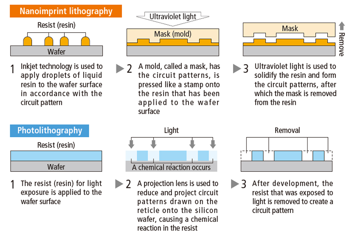
"In contrast to conventional photolithography equipment, which transfers a circuit pattern by projecting it onto the resist coated wafer, the new product does it by pressing a mask imprinted with the circuit pattern on the resist on the wafer like a stamp"
Etching a wafer is only one step in the process, how do they deposit the metal layer? With lithography you have the resist that can be washed away after deposition.
How does any of this stuff really work? It seems as close to magic as I can possibly imagine, the idea that the laser source alone for EUV lithography fires a laser twice at single tiny droplets of falling tin, once to turn the droplet to tin plasma and again to generate the right wavelength of light, all in a fraction of a second, and this happens at up to 50,000 times per second. Seems mad to me...
How do you even create a mask of that size? With photolitography you can at least reduce feature size compared to mask size with the help of lens. But here you need a process capable of making 5nm features (or whatever 5nm actually means) to produce a tool for making 5nm features. Seems a bit like chicken and egg problem. You could do it using photolitogrpahy, but wouldn't that defeat the point?
Is there a manufacturing process which can produce features that small, and is cheap enough for producing masks, but not cost effective for the quantities of producing final product?
The mirror system used to project EUV might be able to do a reduction of the mask image by a small factor, but even so, the size of the features on the mask is too small to allow the production of the masks by photolithography.
As another poster has said, since many years ago the masks are produced by electron-beam lithography, even for traditional UV photolithography.
Electron-beam lithography and ion-beam lithography allow the production of chips with features as small as they can ever be possible (due to atom size constraints), but they make the images too slowly for mass production (because the beam scans sequentially the surface of the wafer), so they can be used only for making masks or for making devices used in research projects, where the cost per device does not matter.
I think the idea is that you only have to make far fewer masks than wafers, so you can make it slowly. I'm sure it's quite difficult to make, and Canon must have been working to get it right for quite some time.
Good to see they haven't given up in their competition with ASML.
Well, you would need a template with 8x smaller features than a EUV mask (at least in one direction, 4x in the other). Ebeam lithography can in principle do this, but it's at the resolution limit and the shot noise will mean there will be a lot of defects.
A sufficiently defect free EUV mask can be worth >>1E6$, for a nano imprint template this would be much much more and it's lifetime probably a fraction.
That's why nanoimprint litho is no alternative to EUV.
Does someone with more knowledge know why this is not used more for chip production? Is it just new, and TSMC is screwed? What are the downsides? Speed?
Edit - thanks for the answers - and yes it would make more sense for ASML to be worried, and TSMC to be happy to not have to use/power/maintain machine that shoot nano-drops of tin with lasers: https://www.trumpf.com/en_US/solutions/applications/euv-lith...
Last time I heard about this tech (~8 years ago, when it was nowhere near commercial availability) that was the obstacle. Since the mask comes into physical contact with each wafer there is unavoidable wear on the mask with each wafer (actually with each chip). So the mask life is a certain number of chips; then you have to make a new one.
Presumably, wouldn’t that still be an improvement in throughout? If a mask can be used to make N chips and time to make a mask is less than the time to laser equivalent chips, you have a win.
Possibly, but masks are very expensive: a full set for a chip on 3nm photolithography reportedly costs >$40M. That's gotta do a lot of chips to not affect the cost of chips drastically. Maybe the masks for this process are cheaper, though?
Is this really such a big issue compared to laser lithography?
Current lithography machines have consumable parts as well (the mirrors below the tin droplets slowly degrade and need to be switched out after a certain amount of use).
In addition, isn't the cost of a mask in it's design, not it's production?
> In addition, isn't the cost of a mask in it's design, not it's production?
They tend to be in the same ballpark.
There's a feedback effect: if the maskset gets cheaper you can afford to do shorter product cycles (think "iphone 15.5"), now you've got two masksets each with half the engineer-years devoted to it. This lets you be a bit bolder with the design since the cost of screwing up is lower. If masks get super-expensive then you only do one maskset and you throw more design-hours into making damn sure it's correct, and spend more time adding in "chicken bits" -- ways to turn off features that you screwed up, without ruining the whole chip -- and fallback options or insurance-policy type stuff. So the design cycle will lengthen or shorten if the engineering cost is several times larger or several times smaller than the mask cost. They sort of balance out.
Also the design cost is often impossible to define exactly. Blocks from previous designs get reused, so you can't really "charge" the effort it took to design them to just one chip. All the major design houses write a lot their own CAD tools too, and these tools have decade-or-longer lifetimes.
Chemistry. Etching is not ideal process. In real life it not make ideally vertical hole, but it tends to go V-like or ^-like, so real mask will have artifacts, which are much narrower or much wider than considered, or sometimes could overlap.
This could been handled by careful selection of parameters - solution concentration, temperature, pressure, mechanical mixing, etc, but on each step of feature size, it become harder to achieve.
I have first education electronics engineer, and I seen broken PCBs, where these artifacts seen by naked eye.
To continue the patterning roadmap, many techniques were considered back in the day, including 157 litho v. NIL v. EUV v. Direct Self Assembly. For NIL, the biggest issue was defect density...why NIL found a niche in disk drive applications (Toshiba early champion) where you have a lot of redundancy built in
Because of EUV's insane cost / complexity, many older litho techniques (NIL, Direct Self Assembly) are making a comeback...NIL is a great option for lower cost patterning applications, like optical/photonic components (Magic Leap etc)
And here I am having just watched some hours-long set of Asianometry video essays in the last year or so about how Japan completely lost the edge in the lithography market.
This uses e-beams to make the mask, right? Edit: here's their research paper (7 years old but note the identical model name FPA-1200NZ2C):
http://cnt.canon.com/wp-content/uploads/2016/08/Nanoimprint-...
Turns out they e-beam a "master mask" and then use that as an imprint to create "replica masks". Then the "replica masks" imprint the wafers. Sadly you still have to start with a crazy-expensive e-beam mask.